Wednesday, 11 December 2013

The future of solar cells?

As mentioned in one of the last posts we had a project at the university last week which we will finish tomorrow with a presentation. In this project we measured the reflectance of nanowire arrays depending on their diameter. What? And why?

One of the most promising energy sources ever is the sun. Solar cells are used to take advantage of this mega-source. But common solar cells are not that efficient. (20 - 30 percent I think.) So some intelligent physicists had the idea to investigate different approaches than using silicon for the cells. Especially here in Lund nanowires are of big interest. And I have to say the guys here are very good (means respected world-wide ;) ) at  growing nanowires. Now what are nanowires and why are they special? The name implies already what is behind the technique: Nanowires are wires with a very small diameter from a few nanometers up to maybe 100 nm. (And yes, this is true, we saw them under a scanning electron microscope!) The special thing about them is that they can be formed out of semimetals that have very nice electrical properties but cannot be used to form layers or bulk samples. This is because if they are present in solid form the distance between their atoms are very different for different metals. That causes strain in the material and this again causes cracks. Not good, solar cell broken. In nanowires this does not happen as the strain from the different atom spacing can be compensated due to the large surface-to-volume ratio of the wires.

Figure 1: Schema of the arrangement of the wires on the sample.
Indium phosphide was used during this project. On the right there
is a schema of the sample that we measured. Each array on the
sample contains nanowires of different diameter.
But back to nanowires in solar cells. As mentioned these semimetal compounds have nice electrical properties which promise higher efficiencies than common solar cells. If they are placed for example in arrays like shown in figure 1 they can - put simply - absorb sunlight which can be used to generate energy. Just like in common solar cells, only more efficient. What we did in the project was to measure the reflectance of such nanowire arrays. If energy is generated by absorbing sunlight it is of course very desirable that the cells/arrays absorb as much of the light as possible. And thus show a reflectance  as low as possible. That was what our measurements were about. We varied the diameter of the nanowires and measured reflectance spectra. Some are shown below (figure 2). Every colour represents a different nanowire diameter and you can see that the reflectances vary depending on the wire diameter.
The reason why the reflectance depends on the diameter is that the absorption and thus the reflection of light depends on how strongly the electromagnetic light fields couple into the nanowires. This again depends on the diameter of the wires so the reflectance depends on the diameter as well. Now only somebody needs to make this applicable for industrial fabrication and here we go - energy crisis solved. ;)

This is very recent research by the way! An extensive paper on this topic which we used to prepare for the project was released only in May this year!

FIgure 2: Reflectance spectra of nanowire arrays. Wavelength on the x-axis,
reflectance on the y-axis. Diameter of the nanowires was varied from 30 nm to 80 nm.
The length of the wires was 1.1 µm.

Thursday, 5 December 2013

Trapped single states

Figure 1: Sample structure: Different
semiconductor materials stacked.
Today I have been working on a lab report all day ... Only after some time I realised how awesome the physics is that is behind the experiment! (At least I think it is awesome. :) ) We trapped single electrons in a quantum well! I mean really single electrons, not the assumed single electrons or only few single electrons. So as I am working on this anyway I thought I should share parts of it in a very high-level (that means not too much crazy science, only a little ;) ) way. I hope it is understandable. :)

The setup consists of a stacked semiconductor structure as shown in figure 1. The gallium arsenide and and the aluminium gallium arsenide have different band gaps which the electrons in the device see as a well in energy. This is like if you jump into a well in the ground - you see the walls around you once you are in the well. (See figure 2 for the wells.)

Figure 2: Two bands resulting from
the different band gaps in the structure
from figure 1 and possible ways
to excite an electron from the bottom
to the top. Laser!
The next prerequisite is to know that physicists assume that there are differen bands in semiconductors that define the energies that electrons can have. (In which they can move if you want.) Now there are not only bands for electrons but also for holes which are the conception of missing electrons. Just like if you take a chocolate marshmallow out of its box leaving a blank space. These holes can move as well just like electrons.
So if there is an electron in one of the bands (the valence band to be precise) it can be moved to another band (the conduction band) by giving energy to it. (For example by shooting at it with a laser - pew, pew!) From before now it is known that this will leave a hole behind.

Figure 3: Spectrum recorded
during the experiment.
After some time the excited electron (the one that was shot to the other band) and the hole recombine because it is more suitable for them. (Particles always want to reach the lowest possible energy state.) If they recombine they emit the energy that the electron got from the laser before. This is visible as light so it can be detected. By a detector ...

Because we are not sure (unless we calculate it before, as I just had to for the lab report ...) which energy this light will have we let the detector detect a lot of possible energies. For some of the detected energies there will be nothing special but for some other energies there will be peaks which means that at these energies there is something going on. For example recombination of electrons and holes. This measurement of different energies is called a spectrum. Figure 3 shows an original spectrum from our experiment. :)

But how do we know that we trapped only one single electron in our well? That we know from the calculations. The movement of particles can be described by the Schrödinger equation. The setup with the quantum well gives boundary conditions to this equation so we get discrete solutions for it. As the semiconductor setup used is a little more complicated than a "normal" quantum well (whatever a >normal >quantum well may be ... <.< ) the solutions for the Schrödinger equation could not be obtained analytically. Instead we used a graphical method. The clue behind this is to plot the graph of the equation. Only at points where the graphs intersect a bound (trapped) state can exist. If you look at figure 4 you see yourself that there is only one intersection point. So one single trapped electron.! BÄM, science! ;)

Figure 4: Graphical solution of the Schrödinger equation. There is only
one intersection point (blue and red) so there is only one(!) single(!) electron
trapped in the quantum well!
So this was a very much broken down overview of what happened. I hope you could understand something. I am still fascinated that something like this is possible and that we did it. O.O

Last thing: Why do we do stuff like this? Well if the behaviour of the electrons in the well is better understood one can build some fancy devices out of this! Maybe new transistors which result in faster computers? Maybe quantum computers? Maybe better solar cells? (Actually I participated in another project where we measured nanowire solar cell arrays! I hope that I will tell something about this as well.)

If I am that fascinated this seems to be the right stuff to study! :)

Thursday, 28 November 2013

The first Swedish snow! And polar lights!

Polar lights! (Green laser, actually ...)
 Yesterday I really saw the first Swedish snow! And even polarlights! Nah ok we created it in the lab. :( But it looked cool nevertheless. ;)

The lab exercise was about Raman spectroscopy and photoluminescence (excitation) spectroscopy. What thaaat?! Well just a short description and then fancy pictures. ;)

In Raman spectroscopy a material is excited with a laser. (This means that electrons absorb energy from the laser and start to dance inside the sample.) After some time the electrons relax to their former state and release their energy from before. So we see a peak at their excitation energy. But apart from that there are more peaks! While dancing the electrons can collide with atom nuclei and give them some of their energy. The lattice then starts to vibrate. This is called a phonon. So now the electrons have less energy than before and of course now they can only emitt less energy. => Another peak. This works the other way around as well so there is another peak with higher energy than before.
SNOOOW!1!

The photoluminescence spectroscopy we did with quantum wells. Small energy valleys in a material. Shooting at the sample with a laser again electrons are lifted to another energy state (conduction band) and at the same time holes (a lacking electron) is created in a lower energy state (valence band). Both of them can be created at almost any level in their respective bands. Afterwards they move to the lowest energy level as all things do and after some more time they recombine. (Electron + missing electron -> electron gone ;) - only in the area where we are looking of course) This again emits energy and that is all the joke about photoluminesence spectroscopy.

With both you can investigate materials. (Solid state) physicists like to do this. ;)

Tuesday, 5 November 2013

Back to brains

Subject of my bachelor thesis:
The Raspberry Pi that replaced the board on the right.
No, this is not another Halloween anecdote but rather a step back to my bachelor time. A few days ago I stumbled upon an article on medicalxpress where it is said that scientists found out that the dendrites in the brain are not mere "wires" as was assumed so far but that they show spiking capabilities as well! This menas that they can actively process and generate information! If this would happen in your PC it would mean that its wires work as processors as well. Sounds great and could bring some interesting properties of the brain with it. It seems to be proven that this plays a role e.g. in the brain's visual activities so this is not another physics gimmick. ;)

Now why is this of special interest to me? As some might remember I wrote my bachelor thesis in this area of research and I did an internship in the same research group in Heidelberg. Still I am not detached of the matter and who knows? Maybe I will do a phd on this subject? ;)

What "my" research group (Electronic Vision(s)) actually does is building a brain based on electrical circuits. Awesome! With this you can perform experiments afterwards and test your theories about how the human brain works. This again can give rise to new computer techniques (which will not only serve the NSA ...), an understanding of brain illnesses and maybe ways to cure them. (The music of future ...) Besides, it would incredibly awesome to understand how a brain works!

In the end of course I have to use this occasion to promote my incredibly steep scientific career at this point and provide you with my bachelor thesis. ;)

A Raspberry Pi controlling neuromorphic hardware - just in case you are interested ... (In any case there are some nice pictures in it!)

Tuesday, 22 October 2013

Most recent stroke of genius by my favourite company!

As some of you might know I am a real Apple fan from the beginning of the first iPhone! So I was very amused when I found the video below on Caschys Blog today. On his youtue channel Vaclav Krejci showed how to design the iOS 7 with only the basic picture editing tools (or rather progressed?) delivered by Microsoft Word. Yes, this programme was developed by this small company that wants to compete with Apple's awesome operating systems ... Ouw ouw, what did Apple do here? :D
A design that simple might not mean anything besides the exorbitant prices, closed up hardware you cannot repair on your own so easily (most recent highlight: Somewhere I read that Apple soldered the processors of the new iMacs onto the socket <.< ) or all the other features I love about my favourite company. :) Nevertheless I found this video funny somehow. ;)

Wednesday, 9 October 2013

Higgs, Higgs, hurrah!

First of all: I borrowed the title of this post from here because I liked it so much. :) Just for the credit ... And sorry for the missing sources, I just wrote down what I remebered. There should be quite some material easily accessable using the search engine of your choice at the moment. ;)

So Peter Higgs and Francois Englert really got the Nobel prize - for predicting a particle that seems to be discovered now. I am not an expert in particle physics although some of my bachelor exam was on this topic. Sometimes it might even be advantageous to not know all the details when explaining something so one does not go too far into details. In the following I will try to give a comprehensible insight into this Higgs stuff ...
CMS detector. ((c) CERN HP)

The Nobel prize this year was awarded for the predicition of the Higgs boson. So first of all: What is a boson? Well, short and simplified version: It is a particle. Then second and third question: What is a prediction and why would someone come up with it?
When theoretical physicists perform their crazy black magic in their super secret "labs" (aka pen + paper on desk) they might come up with so called theories. These theories try to explain phenomena observed by experimental physicists (those are the cool guys with lasers and sh*t ;) ) before and at the same time might predict some stuff that should be possible to observe as well. The last part then is what the experimantalists try to do by throwing around with money and building incredibly complicated toys called particle colliders. In the given case of the Higgs boson the theory of the standard model predicted this special boson and in 2012 it might have been found. So far so good.

But how did this special boson sneak into the standard model? This happened in the beginning of the 1960s when the recent model at the time predicted stuff that was not true like particles having no mass except it was already observed that they have mass or like forces that should exist but do not exist.
Weird stuff.
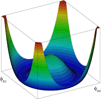
Potential of the Higgs field. (Source: wikipedia)
So some researchers (amongst them Peter Higgs and Francois Englert) came up with the new fancy idea that there could be a field that is everywhere and interacts with particles to give them mass. The new model including this idea predicted stuff that made more sense than before so the physicists went along with it after some time. The only thing that was missing to prove this theory right was the Higgs boson.

This boson is an excitation of the Higgs field mentioned above and it can be measured as a particle with a mass. Now this is really weird again: Excitation of a field? Suddenly a particle? Excitation has mass? What? Let me skip this and just say: If someone found the Higgs boson than there is probably a Higgs field. This seems to have happened in 2012 at the CERN in about the following way: Following Einstein's E = m*c^2 one can clash particles which results in energy. Out of this energy (yes, only the energy and nothing else but E = m*c^2) new particles can form. In this way the physicists at the CERN clashed particles and measured the particles that formed out of the energy afterwards. Easy enough. The reason why it took so long to find the Higgs boson is that it is very heavy so you need much energy to form it. (Transfer task - look at the quation to understand this. ;) ) So the problem was to accelerate the clashing particles fast enough to get this energy.

Yes, physicists like to play in the basement ... LHC collider.
((c) CERN HP)
The last part is then the detection and the question why I always used the subjunctive when writing about the detection of te Higgs boson. If physicists measures something they measure it often. Very often. By that they receive statistical data about their measurements and only if this data meets certain criteria physicists say that it is ok. Some physicists outside CERN still doubt the discovery of the Higgs boson or its existance in general. Partly because they want more measurements. ;) To their credit: It is hard to believe that it has been found as it is some really fundamental small particle.

Monday, 7 October 2013

What physicists do in the lab part II: Nobel Prize!

Tomorrow the nobel prize in physics will be announced! But what for? To show that physicists do not (always) only live in their ivory tower of bubbly dreams I shortly summarised what I remember about the three most promising candidates for the nobel prize in physics 2013 do/did. (Most promising according to thomsonreuters.)
 
Hideo Hosono - Iron-based superconductors


Superconductor floating over a
permanent magnet.
(wikipedia)
Short story for this one: Supraconductive means that a material loses all its electrical resitivity. This is pretty cool because often you do not like resistivity. It costs energy. So everybody is happy when the resistivity is low. (At least in some applications.) For a long time low temperature was required to reach superconductivity. Then someone found somethin about copper-based superconductors at "high" temperatures where high means several Kelvin. (Around  50 - 70 I think - was a nobel prize in 198something as far as I remeber.) Now someone (Hideo Hosono) found something iron-based. Next nobel prize? ;)

Galaxy M51. ((c) MPIA Heidelberg)
Geoffrey W. Marc, Michel Mayor, Didier Queloz - Exoplanets
What do astrophysicists do? Yeees, look for aliens! ;) A very fascinating question not only to physicists is the one if we are alone in the universe ... Philosophers may wonder, religious people may beleive, physicists go looking for it. First step: Find planets outside our solar system. The three guys named above did exactly that. I am not an astrophysicist but I think they managed to do so by examining the planets' bending of light of stars. Pretty cool, huh? ;)

François Englert and Peter W. Higgs - The Higgs Boson
ATLAS detector. ((c) KIP Uni Heidelberg)
Maybe some of you have already heard of this mysterious particle - the "God particle". It is so important to physicists that they have been looking for it since the 1960s when its existance was predicted for the first time. But how can one predict the existance of a particle? Well, most of our modern physics is based on the so called standard model which explains the four fundamental forces (gravitaional, electromagnetical, strong and weak force) with the interaction of different particles. The latter three are quite well explained in this model, only for gravitation there was no corresponding particle. But there should have been one according to the standard model. Thus, physicists tried to find it in order to confirm the correctness of their beloved model. (If they never found/find it they might have to assume that the standard model is wrong - horrible vision!) In March 2013 now some physicists may have found it at the LHC (Large Hadron Collider) in Genf. This discovery might be worth a nobel prize because the standard model and hence the current understanding of physics would have been proven right. (To a certain degree ...)

The procedure of winning a nobel prize can be found here by the way. :)

Friday, 4 October 2013

What physicists do in the lab part I: The plasma microwave and the 30 million euro baking oven

Today we were in the lab again and entered the real clean room. Air filtering, whole-body overall, no cell phones, anti-vibrant floors, no breathing allowed, ... that kind of clean room. And we worked with a plasma microwave. This is not a joke!^^ They used a microwave to build a plasma ashing tool. This etches "stuff" with the use of plasma. (Plasma is a partially ionised gas which glows in the dark - like a lightsabre somehow.) Inside the microwave a plasma is created with the microwave microwaves. The plasma ions then react with the surface you want to etch and remove it. And I just have to repeat: You can build something like this from an ordinary microwave!

Electron Beam Lithography Tool - Lund Nano Lab (image from lecture script)
This wardrobe like or industry baking oven like looking thing is not the plasma microwave. This is an Electron Beam Lithography (EBL) Tool. (I think our teacher mentioned something about 30 million euros ...) What it does is "simply" writing structures on a photo resist with an electron beam.

Why should anybody do such things like writing with the help of electron beams or etching stuff with plasma in a microwave? Well, this time this is not just because we can! Maybe ask your mobil phone or your PC why anybody should do this. ;) These processes are necessary to produce the processors and stuff in all your electronic toys. Would not work without plasma microwaves. ;)

Tuesday, 1 October 2013

3D Tri-Gate Transistor

The title does not refer to one of the Tri-Pod fighting robots from Star Wars Episode III. Rather it refers to the future of transistors. Yes, I admit, it is a little of covered advertising but they invented it, so it should be ok. Only thing I wonder: Why did it take so long to invent something like this? Althoug it has quite some fancy properties it does not look like black magic ...

In the video Mark Bohr, Senior Fellow at Intel, presents the new 3D Tri-Gate Transistor with some nice animations - enjoy! :) (And do not miss the end, there is even a small joke - I hope not only coltish physicists can love about it. ;) )

Friday, 27 September 2013

Building our own iPhone

As some of you might have guessed an iPhone is not what I would build although you can make lots of money with it ... According to some analyses that I found on Caschys Blog the iPhone components cost about 140 EUR and screwing it together makes another 6 EUR. (link) Selling it for a few hundred EUR afterwards earns you quite some cash.

So maybe I would not build an iPhone but I could agree on any other smartphone you can build for 200 EUR and sell it for 600. ;) Starting last week and continuing today and in the next weeks we are basically doing just that in the lab. We are growing transistors. Those are the small magic devices that make your smartphone smart. And your tablet. And your computer. And everything else with electronics. According to Encyclopaedia Britannica transistors are by far the most common human artifact ever produced. (The article is probably not free to view completely - sry! Mabe wikipedia states the same ...) With up to a few billion transistors in every computer CPU this is not hard to believe.

Below there are some pictures we took in the lab with a microscope. You can see two of the main contacts of the transistor. The strucutres are around 20 to 50 µm small. (If you are interested in how a transistor works read below the pictures. :) )
Image 2: Microscope images of transistor structures.
You can clearly see that our smartphone is almost ready. The screwing afterwards is just odds and ends after the transistor growth. ;)


Picture on top: Source (in the middle) and Drain (circle around) contact. The Base contact is still missing and will be added later.


Image 3: Microscope images of transistor structures.
Picture below: Zoomed in. You can see the edges of the structures where they are etched into the photoresist.


If you want to know how a (MOSFET) transistor works here is a short and (hopefully) easy to understand explanation of its basic principle:

Image 3: Schema of a MOSFET transistor.
The green areas in the image to the right contain some charge carriers and the reddish-pink one contains charge carriers of opposing charge. Thus, no current can flow between source and drain if you apply a voltage between them. If you now apply an appropriate voltage at the base contact it will act as one side of a plate capacitor. This will move the charge carriers in the reddish are away from the base and attract carriers of the opposing charge to the base. (There are some few of these in the reddish are as well.) Now there is a so called conduction channel near the base between source and drain. So now a current can flow between source and drain if you apply a voltage here. Maybe you already guessed that this behaviours makes transistors usable as switches. And that is exactly what they are used for in computers, smartphones, tablets, ... (They are all based on binary operations: 0 and 1, off and on - exactly what a simple switch can provide.)

Thursday, 26 September 2013

The next Star Wars will be real!

Uuuh too much going on. :D Science never stops, science never sleeps. On phys.org/ there are two articles today that get science fiction quite close to our present days: Researchers at Harvard and MIT managed to get photons to interact with each other! The physicists of you will know why this is astonishing. For the non-physicists: Photons usually do not do that. Never. But now they suddenly do ... What does that mean? Well, this means light sabre. We will finally get light sabres! Men I have been waiting for this for years. :D What will be next? Spaceshuttles to go to galaxies far far away? Or maybe Pokeballs?

One of the things that will be next quite certainly is a Star Wars kind of thing as well: Processors made out of carbon nanotubes. (Stanford this time.) Short version: They have the potential to be way faster than current processors and consume less energy at the same time. Sounds too good to be true, right?

The smartest mind of our time

Who might that be? Maybe you guessed it: It is Stephen Hawkings. (At least I would say so. ;) ) Today I found an artivle on gizmodo where they posted a video by The Guardian in which they again summarized Stephen Hawking's work in a nice and simple animation! Take a look, it might change your view on the world. :) If you do not get it at first sight, do not worry - watch it again! After all, this was devised by the smartest mind of our time.

Wednesday, 25 September 2013

YouTube going facebook - or useful?

One of the biggest parts of the internet 2.0 - if not the symbol of the internet 2.0 - is youtube: a video portal where you can find videos about everything. And watch them, of course. But youtube works the other way around as well. Youtube watches you. Starting this week all of you will notice this more than ever before. Yesterday google announced on their official youtube blog that they will change the commenting system for youtube based on your preferences, your interests, your friends. Sounds promising. Probably there will not even be any more cookies or spies watching you as before. (As everything google needs they get from you at the moment anyway ...) So is this the end of flame wars, haters and stupid comments in general? Or is it another infringement on your freedom on the internet? What do you think?

Monday, 23 September 2013

Shattered study dreams ...

The title of this post might be a little misleading because what is really behind it is a quite sensational progress in data handling - although it has been already a while: IBM managed to store one bit of information with the bare use of twelve atoms - instead of the usual one million that are used on conventional hard drives. Pretty awesome, only - that is what I wanted to engineer after studying some nanoscience ... Well, then I will probably go back to the teleporter - might be interesting to start with as well. Or maybe one electron - one bit. We will see ...

In any case here is a 3 minute video summing up the story and explaining how it works - understandable for everybody (I hope ... ask, if not. :) )


In addition, here is the IBM link (you can find the video there as well in case the one on this page does not work) and here is the official press announcement from 12 January 2012.